RF Wattmeter and Band Decoder
RF SWR\Wattmeter V1 PCB Version
Posted April 2022
RF tolerant PCB
I updated the code (published on GitHub) to run on a newly designed PCB which has several small configuration changes.
RF-Power-Meter-V1/RF_Wattmeter_Teensy41_PCB_V1 at master · K7MDL2/RF-Power-Meter-V1 (github.com)
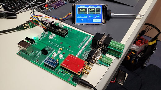
The prototype had lots of wire jumpers, all are antennas. My device is located outdoors, connected via ethernet near the 5-band VHF transverter, several VHF antennas, and high power VHF amplifiers. I had problems with 100W on 144Mhz pointed at it. The CPU would lock up and the amps would be stuck in transmit (with no RF). I added lots of ferrite beads and a watchdog card to reboot it after 40 seconds as a workaround. I run up to 500W only 20ft away.
In March 2022 I designed a PCB with optocouplers located close to the IO connectors, board edge connectors, and no wires except the cabling to the combo USB/Enet jack (now are traces on the V2 board) and short lines to the optional Nextion touchscreen or small OLED displays. The power and data lines for those are EMI filtered. Band decoder line inputs to optocouplers are filtered and have isolated power and ground supplied by the radio side. The PCB was sized to slide into a common online sourced aluminum box for shielding. It does have mounting holes to fit into any suitable sized box.
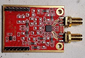
Below is the Assembled V1 PCB. The red module is the SV1AFN ADL5519 10GHz dual log detector. It features a wide range linear output (in dB) with both detectors closely matched. Being on the same chip, temperature affects both equally. I read the temperature output for a convenient way to get an approximate ambient temp in my outdoor cabinet. It has internal temperature compensation but you can use the temperature output to further calibrate the detectors. I find this unnecessary. I have calibration values for each band, which may have a shared or independent coupler switched onto the detector inputs. It provide very accurate values.


I removed the external watchdog card after finding new Teensy 4 code to control the internal watchdog capability. This seems to work and saves the cost and wiring of a separate card.
As I built the V1 PCB I fixed the trace errors and improved several items, one being wider IO connector spacing to allow clearance for hoods on the D-Sub connectors. I routed traces for the USB and Enet combo jack. I added a low power 12V to pin 15 of each D15 output port connector to power low current relay or drivers. Keep in mind the input pico-fuse sizing and the nearby reverse polarity protection diode current capability when loading this 12V source. I am using a 1.5A pico fuse soldered in. You could install a socket for this fuse.
The only internal wires are now the 4 lines to the OLED display or Nextion display (if used). I have not built V2 but the files are posted on GitHub. I have several more V1 boards if anyone wants to build one. It uses about 14 dual optocouplers, a Teensy 4.1, ADL5519 10GHz log dual detector, and a ADS1115 4ch 16bit ADC i2c module, same as the previous hand wired version. Now the modules all plug into the PCB.
The V1 board has a couple small PCB trace errors easily fixed and the PCB is now in service outside working with 500W on 2M nearby no problem. The problems were:
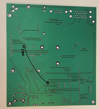
1. Missing 3.3V to the ADS1115 ADC module jack. See photo below with black line showing where to connect a jumper wire.
2. A short vertical trace for 3.3V to Pin 1 of J13 was on the wrong PCB side shorting 2 top side horizontal input traces from the same connector. Cut the vertical trace in 3 places to isolate the 2 horizontal traces. This 3.3V trace is not used. See picture below showing the trace cuts.
3. The footprint for the input diode is too small for most diodes anyone would use. Scrape off solder mask on the +12V trace as needed to land one end of the chosen diode on it. This and a few other footprints were optimized on the V2 board.
4. The ethernet 2x3 pin header next to the Combo jack is 1mm pitch, should have been 2mm pitch. I used the 6 conductor ribbon cable from the optional Teensy Enet kit and cut of one connector and soldered the wire ends into the holes. This requires a light touch with the soldering iron to prevent melting the wire insulation and having shorts. The V2 board is now using traces, same for the USB host jack which is not used in this project.
I have not built a V2 board as I still have several V1 boards that work fine.